
具体描述
内容简介
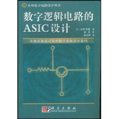
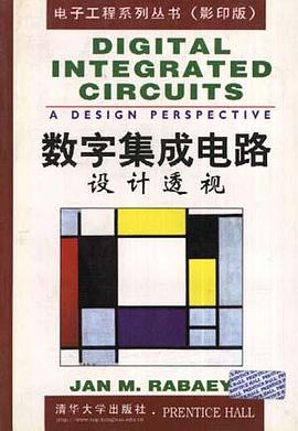
市面上虽然已有许多关于数字集成电路设计的书籍,但
绝大部分都是孤立地讨论“数字系统”、或“数字电路单元”、
或“设计方法”。而本书则将系统、电路和设计方法这三者
有机地结合起来,深入地讨论了CMOS、双极型和砷化镓
(GaAS)数字集成电路。本书在详细介绍集成电路的器件模型
和墓本单元电路的基础上,系统地介绍了数字集成电路系统
设计中的四类关键技术:运算单元设计、时序组织与规划、
存储单元、互连线与寄生效应,是一本内容丰富,且特别
适合于深亚微米数字集成电路设计的优秀教材。
作者简介
目录信息
Chapterl: Introduction
1.1 A Historical Perspective
1.2 Issues in Digital Integrated Circuit Design
1.3 To Probe Further
1.4 Exercises
PART 1: A CIRCUIT PERSPECTIVE
Chapter 2: The Devices
2.1 Introduction
2.2 The Diode
2.2.1 A First Glance at the Device
2.2.2 Static Behavior
2.2.3 Dynamic, or Transient, Behavior
2.2.4 The Actual Diode-Secondary Effects
2.2.5 The SPICE Diode Model
2.3 The MOS(FET) Transistor
2.3.1 A First Glance at the Device
2.3.2 Static Behavior
2.3.3 Dynamic Behavior
2.3.4 The Actual MOS Transistor-Secondary Effects
2.3.5 SPICE Models for the MOS Transistor
2.4 The Bipolar Transistor
2.4.1 A First Glance at the Device
2.4.2 Stalic Behavior
2.4.3 Dynamic Behavior
2.4.4 The Actual Bipolar Transistor-Secondary Effects
2.4.5 SPICE Models for the Bipolar Transistor
2.5 A Word on Process Variations
2.6 Perspective: Future Device Developments
2.7 Summary
2.8 To Probe Further
2.9 Exercises and Design Problems
Appendlx A: Layout Design Rules
Appendlx B: Small-Slgnal Models
Chapter 3: The Inverter
3.1 Introduction
3.2 Delinitions and Properties
3.2.1 Area and Complexity
3.2.2 Functionality and Robustness: The Static Behavior
3.2.3 Performance: The Dynamic Behavior
3.2.4 Power and Energy Consumption
3.3 The Static CMOS Invener
3.3.1 A First Glance
3.3.2 Evaluating the Robustness of the CMOS Inverter: The Static Behavior
3.3.3 Perfonnance of CMOS Inverter: The Dynamic Behavior
3.3.4 Power Consumption and Power-Delay Product
3.3.5 A Look into the Future: Effects of Technology Scaling
3.4 The Bipolar ECL Inverter
3.4.1 Issues in Bipolar Digital Design: A Case Study
3.4.2 The Emitter-Coupled Logic (ECL) Gate at a Glance
3.4.3 Robustness and Noise Immunity: The Steady-State Characteristics
3.4.4 ECL Switching Speed: Thc Transient Behavior
3.4.5 Power Consumption
3.4.6 Looking Ahead: Scaling the Technology
3.5 Perspective: Area, Perfonnance, and Dissipation
3.6 Summary
3.7 To Probe Further
3.8 Exercises and Design Problems
Chapter 4: Designing Combinational Logk Cates in CMOS
4.1 Introduction
4.2 Static CMOS Design
4.2.1 Complementary CMOS
4.2.2 Ratioed Logic
4.2.3 Pass-Transistor Logic
4.3 Dynamic CMOS Design
4.3.1 Dynamic Logic: Basic Principles
4.3.2 Perfonnance of Dynamic Logic
4.3.3 Noise Considerations in Dynamic Design
4.3.4 Cascading Dynamic Gates
4.4 Power Consumption in CMOS Gates
4.4.1 Switching Activity of a Logic Gate
4.4.2 Glitching in Static CMOS Circuits
4.4.3 Short-Circuit Currents in Static CMOS Circuits
4.4.4 Analyzing Power Consumption Using SPICE
4.4.5 Low-Power CMOS Design
4.5 Perspective: How to Choose a Logic Style
4.6 Summary
4.7 To Probe Further
4.8 Exercises and Design Problems
Appendix C: Layout Techniques for Complex Cates
Chapter 5: Very High Perfonnance Digital Circuits
5.1 Introduction
5.2 Bipolar Gate Design
5.2.1 Logic Design in ECL
5.2.2 Differential ECL
5.2.3 Current Mode Logic
5:2.4 ECL with Active Pull-Downs
5.2.5 Altemative Bipolar Logic Styles
5.3 The BiCMOS Approach
5.3.1 The BiCMOS Gate at a Glance
5.3.2 The Static Behavior and Robustness Issues
5.3.3 Perfonnance of the BiCMOS Inverter
5.3.4 Power Consumption
5.3.5 Technology Scaling
5.3.6 Designing BiCMOS Digital Gates
5.4 Digital Gallium Arsenide Design *
5.4.1 GaAs Devices and Their Properties
5.4.2 GaAs Digital Circuit Design
5.5 Low-Temperature Digital Circuits *
5.5.1 Low-Temperature Silicon Digital Circuits
5.5.2 Superconducting Logic Circuits
5.6 Perspective: When to Use High-Performance Technologies
5.7 Summary
5.8 To Probe Further
5.9 Exercises and Design Problems
Appendlx D: The Schottky-Bamer Oiode
Chapter 6: Designing Sequential Logic Circuits
6.1 Introduction
6.2 Static Sequential Circuits
6.2.1 Bistability
6.2.2 Flip-Flop Classification
6.2.3 Master-Slave and Edge-Triggered FFs
6.2.4 CMOS Static Flip-Flops
6.2.5 Bipolar Static Flip-Flops
6.3 Dynamic Sequentia) Circuits
6.3.1 The Pseudostatic Latch
6.3.2 The Dynamic Two-Phase Flip-Flop
6.3.3 The C2MOS Latch
6.3.4 NORA-CMOS-A Logic Style for Pipelined Structures
6.3.5 True Single-Phase Clocked Logic (TSPCL)
6.4 Non-Bistable Sequential Circuits
6.4.1 The Schmitt Trigger
6.4.2 Monostable Sequential Circuits
6.4.3 Astable Circuits
6.5 Perspective: Choosing a Clocking Strategy
6.6 Summary
6.7 To Probe Funher
6.8 Exercises and Design Problems
PART 11: A SYSTEMS PERSPECTIVE
Chapter 7: Designing Arithmetic Building Blocks
7.1 Introduction
7.2 Datapaths in Digital Processor Architectures
7.3 The Adder
7.3.1 The Binary Adder: Definitions
7.3.2 The Full Adder: Circuit Design Considerations
7.3.3 The Binary Adder: Logic Design Considerations
7.4 The Multiplier
7.4.1 The Multiplier: Definitions
7.4.2 The Array Multiplier
7.4.3 Other Multiplier Structures
7.5 The Shifter
7.5.1 BarrelShifter
7.5.2 Logarithmic Shifter
7.6 Other Arithmetic Operators
7.7 Power Considerations in Datapath Structures
7.7.1 Reducing the Supply Voltage
7.7.2 Reducing the Effective Capacitance
7.8 Perspective: De.sign as aTrade-off
7.9 Summary
7.10 To Probe Further
7.11 Exercises and Design Problems
Appendix E: From Datapath Schematics to Layout
Chapter 8: Coping wlth Interconnect
8.1 Introduction
8.2 Capacitive Parasitics
8.2.1 Modeling Interconnect Capacitance
8.2.2 Capacitance and Reliability-Cross Talk
8.2.3 Capacitance and Performance in CMOS
8.2.4 Capacitance and Performance in Bipolar Design
8.3 Resistive Parasitics
8.3.1 Modeling and Scaling of Interconnect Resistance
8.3.2 Resistance and Reliability-Ohmic Voltage Drop
8.3.3 Electromigration
8.3.4 Resistance and Performance-RC Delay
8.4 Inductive Parasitics
8.4.1 Sources of Parasitic Inductances
8.4.2 Inductance and Reliability- Voltage Drop
8.4.3 Inductance and Performance-Transmission Lin5e Effects
8.5 Comments on Packaging Technology
8.5.1 Package Materials
8.5.2 Interconnect Levels
8.5.3 Thennal Considerations in Packaging
8.6 Perspective: When to Consider Interconnect Parasitics
8.7 Chapter Summary
8.8 To Probe Further
8.9 Exercises and Design Problems
Chapter 9: Timing Issues in Digital Circuits
9.1 Introduction
9.2 Clock Skew and Sequential Circuit Performance
9.2.1 Single-Phase Edge-Triggered Clocking
9.2.2 Two-Phase Master-Slave Clocking
9.2.3 Other Clocking Styles
9.2.4 How to Counter Clock Skew Problems
9.2.5 Case Study-The Digital Alpha 21164 Microprocessor
9.3 Self-Timed Circuit Design*
9.3.1 Selt-Timed Concept
9.3.2 Completion-Signal Generation
9.3.3 Self-Timed Signaling
9.4 Synchronizers and Arbiters*
9.4.1 Synchronizers-Concept and Implementation
9.4.2 Arbiters
9.5 Clock Generation and Synchronization*
9.5.1 Clock Generators
9.5.2 Synchronization at the System Level
9.6 Perspective: Synchronous versus Asynchronous Design
9.7 Summary
9.8 To Probe Further
9.9 Exerci.ses and Design Problems
Chapter 10: Designing Memory and Array Structures
10.1 Introduction
10.2 Semiconductor Memories--An Introduction
10.2.1 Memory Classification
10.2.2 Memory Architectures and Building Blocks
10.3 The Memory Core
10.3.1 Read-Only Memories
10.3.2 Nonvolati le Read-Write Memories
10.3.3 Read-Write Memories (RAM)
10.4 Memory Peripheral Circuitry
10.4.1 The Address Decoders
10.4.2 Sense Amplifiers
10.4.3 Drivers/Buffers
10.4.4 Timing and Control
10.5 Memory Reliability and Yield
10.5.1 Signal-To-Noise Ratio
10.5.2 Memory yield
10.6 Case Studies in Memory Design
10.6.1 The Programmable Logic Array (PLA)
10.6.2 A 4 Mbit SRAM
10.7 Perspective: Semiconductor Memory Trends and Evolutions
10.8 Summary
10.9 To Probe Further
10.10 Exercises and Design Problems
Chapterll: Deslgn Methodologles
11.1 Introduction
11.2 Design Analysis and Simulation
11.2.1 Representing Digital Data as a Continuous Entity
11.2.2 Representing Data as a Discrete Entity
11.2.3 Using Higher-Level Data Models
11.3 Design Verification
11.3.1 Electrical Verification
11.3.2 Timing Verification
11.3.3 Functional (or Fonnal) Verification
11.4 Implementation Approaches
11.4.1 Custom Circuit Design
11.4.2 Cell-Based Design Methodology
11.4.3 Anay-Based Implementation Approaches
11.5 Design Synthesis
11.5.1 Circuit Synthesis
11.5.2 Logic Synthesis
11.5.3 Architecture Synthesis
11.6 Validation and Testing of Manufactured Circuits
11.6.1 TestProcedure
11.6.2 Design for Testability
11.6.3 Test-Pattem Generation
11.7 Perspective and Summary
11.8 To Probe Further
11.9 Exercises and Design Problems
Problem Solutions
· · · · · · (收起)
读后感
要读这本书,我觉得得要有三个前提。第一:不急躁的心态,第二:有层次想当的人可以讨论;第三:比较深厚的数字电路的基础。这可能是由于国外的教学方式与国内的教学方式不同,所以造成了国外教材在国内并不被很多学生所接受的原因之一。国外是一种讨论式、引导式的教学方式,...
要读这本书,我觉得得要有三个前提。第一:不急躁的心态,第二:有层次想当的人可以讨论;第三:比较深厚的数字电路的基础。这可能是由于国外的教学方式与国内的教学方式不同,所以造成了国外教材在国内并不被很多学生所接受的原因之一。国外是一种讨论式、引导式的教学方式,...
要读这本书,我觉得得要有三个前提。第一:不急躁的心态,第二:有层次想当的人可以讨论;第三:比较深厚的数字电路的基础。这可能是由于国外的教学方式与国内的教学方式不同,所以造成了国外教材在国内并不被很多学生所接受的原因之一。国外是一种讨论式、引导式的教学方式,...
要读这本书,我觉得得要有三个前提。第一:不急躁的心态,第二:有层次想当的人可以讨论;第三:比较深厚的数字电路的基础。这可能是由于国外的教学方式与国内的教学方式不同,所以造成了国外教材在国内并不被很多学生所接受的原因之一。国外是一种讨论式、引导式的教学方式,...
要读这本书,我觉得得要有三个前提。第一:不急躁的心态,第二:有层次想当的人可以讨论;第三:比较深厚的数字电路的基础。这可能是由于国外的教学方式与国内的教学方式不同,所以造成了国外教材在国内并不被很多学生所接受的原因之一。国外是一种讨论式、引导式的教学方式,...
用户评价
这本书的作者的语言风格非常严谨,这本身是优点,但在这里却成了阻碍。他似乎对“精确”二字有着近乎偏执的追求,导致行文逻辑非常复杂,句子结构冗长且充满了各种从句和限定词。阅读过程中,我需要反复回溯前面的内容,才能确认某一个限定条件到底作用于哪个参数。这种“学术化”的表达方式,虽然保证了定义的严密性,却极大地降低了信息传递的效率。我感觉我不是在学习设计知识,而是在破解一道复杂的语言谜题。一个好的技术书籍应该像一个耐心的导师,引导你清晰地理解概念,而不是像一份冗长晦涩的法律文件,需要专业的“翻译”才能被理解。这种表达上的障碍,使得很多本应直观的知识点变得难以消化。
这本书的排版和插图设计实在让人不敢恭维,这对于一本旨在“透视”复杂电路的书来说,是一个致命的伤。很多关键的电路图看起来模糊不清,线条交叉在一起,让人眼花缭乱,根本无法清晰地分辨信号流向和逻辑关系。更别提那些试图解释复杂概念的示意图了,它们往往过于简化,甚至在某些关键点上存在误导性。阅读体验非常糟糕,我不得不频繁地放大、调整屏幕亮度,才能勉强跟上作者的思路。在数字集成电路这个领域,视觉化的辅助至关重要,它能帮助我们直观地理解时间延迟、功耗分布和面积优化这些核心问题。遗憾的是,这本书在这方面做得非常不到位,让人感觉像是拿着一本早期的技术文档在阅读,而不是一本面向现代工程师的专业书籍。如果能投入更多资源进行高质量的图形设计和排版优化,这本书的阅读体验和知识吸收效率都会有质的飞跃。
拿到这本书时,我满怀期待,希望它能为我打开数字电路设计领域的一扇新窗。然而,读完后我却感到有些失落。这本书的叙述方式过于抽象,仿佛在试图用数学公式构建起整个世界,却忽略了实际工程中的“人”的体验。它花了大量篇幅讲解各种抽象的模型和理论推导,这些内容固然重要,但对于一个初学者或者希望快速应用知识的工程师来说,显得有些晦涩难懂。书中缺乏生动的案例分析,很多时候我需要跳出书本,去外部资源搜索相关的实际应用场景,才能真正理解书中所述概念的意义。如果作者能在理论和实践之间搭建更坚实的桥梁,比如多引用一些行业内的经典设计案例,或者提供更贴近实际的仿真结果,这本书的价值会大大提升。目前的版本更像是一本理论参考手册,而不是一本可以引导实践的“透视”之作。我希望下一版能更注重“设计”的“透视”感,少一些纯粹的公式堆砌。
我特别关注了书中对于现代EDA工具流程的介绍,这是我非常看重的一个环节,毕竟现代IC设计已经完全离不开自动化工具链。然而,这本书在这部分的内容更新明显滞后了。它描述的流程和工具链仿佛还停留在十年前的水平,对于目前主流的布局布线、静态时序分析(STA)以及形式验证等环节的最新发展趋势几乎没有提及。对于如何利用先进的PPA(性能、功耗、面积)优化算法,以及如何应对先进工艺节点带来的设计挑战,书中的论述显得力不从心。对于希望通过这本书来跟上行业前沿的读者来说,这无疑是一个巨大的缺陷。一本关于“设计”的书,如果不能反映当前行业的主流实践和最新技术栈,其时效性和指导价值就会大打折扣。
关于这本书的深度,我持保留态度。它似乎在试图覆盖太多的主题,结果导致每个部分都只是蜻蜓点水,没有真正深入到核心的“设计透视”层面。从CMOS器件原理讲起,到逻辑门设计,再到系统级架构,所有内容都浅尝辄止。例如,在谈及亚阈值功耗管理时,书中只是简单罗列了几种方法,却完全没有探讨不同工艺节点下各种方法的权衡取舍(Trade-offs),比如在速度、面积和泄漏电流之间的动态平衡。对于一个有经验的工程师而言,这些权衡才是设计真正的精髓所在。这本书更像是对现有知识点的快速回顾,而不是提供一种全新的、更深刻的洞察视角。它缺少那种“原来如此!”的顿悟时刻,总觉得总在门外徘徊,无法真正窥见设计背后的深层逻辑和关键决策点。
有讲到完整的电路设计流程,清华教材之一
有讲到完整的电路设计流程,清华教材之一
研究生读过的书。。。。
研究生读过的书。。。。
研究生读过的书。。。。